Menu

 WhatsApp
New Standard: GUIDE TO DEFECTS FOUND ON MONOCRYSTALLINE SILICON CARBIDE SUBSTRATES 1 Purpose The purpose of this guide is to list, illustrate and provide reference for various characteristic features and defects that are seen on silicon carbide wafers. Recommended practices for observation are referenced as far as available standards. The artifacts described in this
WhatsApp 
Polycrystalline silicon, or multicrystalline silicon, also called polysilicon or polySi, is a high purity, polycrystalline form of silicon, used as a raw material by the solar photovoltaic and electronics industry.. Polysilicon is produced from metallurgical grade silicon by a chemical purification process, called the Siemens process. This process involves distillation of volatile silicon
WhatsApp 
Monocrystalline silicon, more often called singlecrystal silicon, in short mono cSi or monoSi, is the base material for siliconbased discrete components and integrated circuits used in virtually all modern electronic equipment. MonoSi also serves as a photovoltaic, lightabsorbing material in the manufacture of solar cells.. It consists of silicon in which the crystal lattice of the
WhatsApp 
Monocrystalline silicon carbide nanoelectromechanical systems Y. T. Yang, K. L. Ekinci, X. M. H. Huang, L. M. Schiavone, and M. L. Roukesa) Condensed Matter Physics 11436, California Institute of Technology, Pasadena, California 91125 C. A. Zorman and M. Mehregany Department of Electrical Engineering and Computer Science, Case Western Reserve University, Cleveland, Ohio 44106
WhatsApp 
monocrystalline silicon carbide plant; 2 Sep 2014 . used portable crushing plant for sale philippines .. used portable rock crusher plant for sale in spain by Read more. Monocrystalline Fused Alumina, Single Crystal Fused .. White Fused Alumina, Silicon Carbide, Garnet, Boron Carbide . Contact Supplier Contact Monocrystalline fused alumina. Henan Ruishi Abrasive
WhatsApp 
The present invention provides an epitaxial SiC monocrystalline substrate having a high quality epitaxial film suppressed in occurrence of step bunching in epitaxial growth using a substrate with an off angle of 6° or less and a method of production of the same, that is, an epitaxial silicon carbide monocrystalline substrate comprised of a silicon carbide monocrystalline substrate with an off
WhatsApp 
Silicon carbide SiC is a compound mainly formed by the covalent bond between silicon (Si) and carbon (C). Its basic unit is siC tetredron, in which Si atom is located in the center and C atom is around. All structures of SiC consist of SiC tetredrons piled up in different ways. Now have found the silicon carbide homogeneity of different crystal structure has more than 200, including the
WhatsApp 
Highly scalable plant will meet growing demand for high quality silicon carbide material HUDSON,, June 27, 2018 (GLOBE NEWSWIRE) GTAT Corporation (GTAT) opened its new stateoftheart
WhatsApp 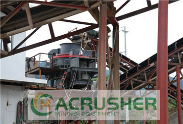
Monocrystalline Silicon. Monocrystalline silicon is chemically etched using strong bases such as KOH, EDP, TM, etc., with etch rates that are highly dependent on the crystalline orientation, etching solution concentration, temperature and doping concentration of etched substrates, shape of masks and relative orientation of masks with respect to the crystal orientation.
WhatsApp 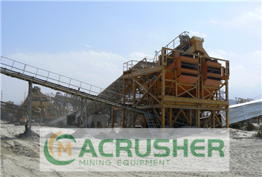
ULTRIGH Q MONOCRYSTALLINE SILICON CARBIDE DISK RESONATORS ANCHORED UPON A PHONONIC CRYSTAL Jeremy Yang, Benoit Hamelin, SeungDeok Ko, and Farrokh Ayazi Georgia Institute of Technology, Atlanta, Georgia, USA ABSTRACT This work introduces a 3D design incorporating a phononic crystal to decouple a centrallysupported silicon carbide bulk acoustic wave
WhatsApp 
CARBOREX® silicon carbide (SiC) is a material with many excellent properties like high hardness and wear resistance, low specific density, an outstanding chemical inertness even at elevated temperatures, high thermal conductivity, low thermal expansion and good shock resistance.
WhatsApp 
Silicon carbide is a material that offers advantages such as improved efficiency for fast powerswitching applications, including hightemperature and highvoltage applications. Initially a solarfocused company, GTAT had expanded its manufacturing processes to include sapphire as way to diversify its product offerings. Last year, the company told NH Business Review it had attempted to thwart
WhatsApp 
The invention relates to a grower of a highpurity semiinsulating silicon carbide single crystal, belonging to the field of crystal growth. The grower comprises a vacuum chamber, a graphite crucible and an induction coil. The grower of the invention is used for growing the highpurity semiinsulating silicon carbide single crystal based on the technology of physical vapor transport (PVT
WhatsApp 
An investigation was conducted to explore the mechanisms of the scratching of monocrystalline silicon carbide with a single diamond grit. The scratching was repeated on a silicon carbide workpiece to generate different wear shapes of the diamond grit. The forces were recorded during each scratching and the wear of the diamond grit together with the silicon carbide morphologies was monitored at a
WhatsApp 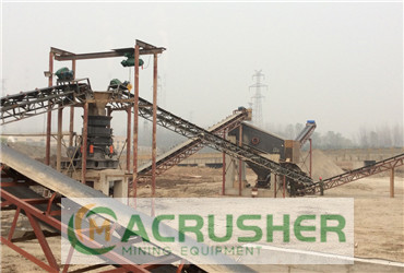
Vibrating Feeder is a linear direction of transport equipment, ore and rock plants, it can send the material crushing uniform continuous. 1; 2; 3; About Us. SHANGHAI AC MACHINERY CO., LTD is one hightech enterprise, which involves RD, production, sales and service as well. In the past 20 years, we devote to producing quarry crushers, sand making machines and industrial grinding mills
WhatsApp 
SiC is an extremely promising material for nanoelectromechanical systems given its large Young''s modulus and robust surface properties. We have patterned nanometer scale electromechanical resonators from singlecrystal 3CSiC layers grown epitaxially upon Si substrates. A surface nanomachining process is described that involves electron beam lithography followed by dry
WhatsApp 
Graphene (/ ˈ ɡ r æ f iː n /) is an allotrope of carbon consisting of a single layer of atoms arranged in a twodimensional honeycomb lattice. The name is a portmanteau of "graphite" and the suffix ene, reflecting the fact that the graphite allotrope of carbon consists of stacked graphene layers.. Each atom in a graphene sheet is connected to its three nearest neighbors by a σbond, and
WhatsApp 
Provided is a monocrystalline silicon carbide ingot containing a dopant element, wherein a maximum concentration of the dopant element is less than 5×10 17 atoms/cm 3 and the maximum concentration is 50 times or less than that of a minimum concentration of the dopant element. Also provided is a monocrystalline silicon carbide wafer made by cutting and polishing the monocrystalline silicon
WhatsApp 
silicon carbide epitaxial growth monocrystalline silicon phase epitaxial Prior art date Legal status (The legal status is an assumption and is not a legal conclusion. Google has not performed a legal analysis and makes no representation as to the accuracy of the status listed.) Granted Application number Other languages
WhatsApp 
CARBOREX® Green is a high purity, semifriable, medium density, green silicon carbide. Silicon carbide is an extremely hard material (Mohs hardness ), is chemically inert and does not melt. Silicon Carbide has a high thermal conductivity, a low coefficient of thermal expansion, is thermal shock and abrasion resistant and has strength at high temperatures
WhatsApp 
monocrystalline silicon carbide wafers for high power and high frequency applications. 2 Scope The complete specification for this product includes all general requirements of SEMI M55. The available quality options are intended to reflect the market at the time of publication of this document. Requirements represent market capability at the time of publication of the standard. NOTICE
WhatsApp 
Download Citation | On Dec 21, 2015, S. V. Ivenin published MONOCRYSTALLINE SILICON CARBIDE WAFERS PROCESSING | Find, read and cite all the research you need on ResearchGate
WhatsApp 
Silicon carbide light emitting diode having a pn junction: : Suzuki et al. : Semiconductor laser using fiveelement compound semiconductor: : Hatano et al. : Blue light emitting diode formed in silicon carbide: : Edmond: : Method for producing semiconductive single crystal: : Taguchi
WhatsApp 
Plane can be defined in terms of intercepts along 3 unit cell axes. + + =1 a b g x y z. File: ee4494 silicon revised 09/11/2001 copyright james t yardley 2001 Page 8 Miller indexes that define plane are inverse of α, β, γ : h, k, l . The plane is then designated (hkl). The set of symmetrically equivalent planes is designated {hkl}. The direction normal to the plane is often
WhatsApp  الصفحة الرئيسية
 معلومات عنا
 اتصل
اتصل