Menu

 WhatsApp
08/06/2018· Since China''s ban on the import of various scrap materials. A lot of countries began to recycle and process the scrap by themselves. Take electronic boards f
WhatsApp 
PCB design is concerned with the process of creating the plans for a printed circuit board. It is different from PCB manufacturing. In PCB design, you learn about the tools, process, and guidelines useful for creating such plans. In PCB manufacturing, on the other hand, you are concerned about the process of converting the plans of a PCB into the actual PCB.
WhatsApp 
Printed Circuit Board. The most vital element in electronic circuits and equipment is the Printed Circuit Board (PCB). It is also possible to build an electronic circuit with breadboards and zero boards, but the method is a low level and less efficient one wherein the designing circuit is prone to damage and the designing involves a complex process of placing the components of the circuit.
WhatsApp 
For easy of understanding the basic Printed Circuit Board Design Process, please go through the following stepbystep procedures of designing a PCB board: Printed Circuit Board Design Process with a Software. StepByStep Procedure: Use any Good EDA (Electronic Design Automation) Tools to Capture Schematic. Keeping in Mind the Type of PCB and Required Circuit, select the Card
WhatsApp 
Crushing The primary crushers located at the open pit mine site, receive ore and waste at separate times. They break the larger rocks down to a size suitable for transport on the conveyor belt. See more detail on crushing. 3. Transport A rubber belted conveyor transports the ore and waste rock from the open pit, approximately two kilometres, via a tunnel through Union Hill, to the mill and
WhatsApp 
16/05/2018· 3 ton/hr Scrap Copper Aluminum Radiator Recycling Plant_Radiator Crushing and Separating Process Duration: 2:29. Ewaste Recycling Machinery 16,575 views 2:29
WhatsApp 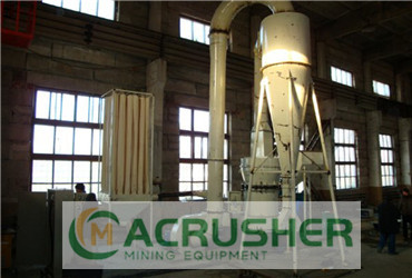
02/02/2017· Saws – Slicing through a PCB with a saw is destructive to the individual board, but can provide valuable insight into the bigger picture of the overall assembly process. Automated Optical Inspection (AOI) – AOI systems are available in cheap and commercial grades. Cheap AOI systems utilize inexpensive webcams in conjunction with Open Source
WhatsApp 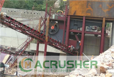
The PCB crushing and separating machinery is used to process the separation of metal and nonmetal in waste printed circuit boards, copper clad laminate, circuit boards and leftover materials, then reuse the copper and resin powder. The equipment uses high voltage electrostatic separator to make the separation more fine, effectively control the loss of nonferrous metals.
WhatsApp 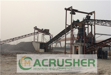
Bittele''s qualified engineers follow defined steps in the PCB assembly process. Our PCB assembly process include preparing the circuit board''s surface, placing the parts, soldering, cleaning and inspection testing. Our trained assembly technicians diligently follow defined procedures and use modern methods of component placement for circuit board assembly. We use both automated and
WhatsApp 
Printed Circuit Board Prototyping Process PCB Flying Probe Test (FPT) PCB Automated Optical Inspection (AOI) PCB Fiducial Mark and Alignment PCB Fusion and Lamination Technology Process A Comprehensive Introduction of Copper Clad Laminate Venn diagram and Sets. Analysis on Plating Copper Process for PCB. The Printed Circuit Boards (PCBs) are a junction of electrical traces and
WhatsApp 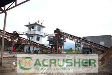
Owing to complicated structure of structure of multilayer PCBs, once problems are observed in the process of subsequent unit module assembly testing, it''s difficult to position breakdowns a result, inspection of their quality and reliability has to be very strict. Apart from regular inspection items mentioned above, other inspection items include the following parameters
WhatsApp 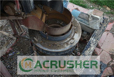
The procedure of crushing the stone has three stages. The first stage is breaking down the stone to small sizes. The second stage is crushing down the sizable stones to suit a specific purpose. On the third stage, the stones are screened for finished products.
WhatsApp 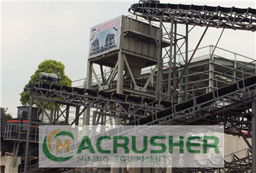
Procedure for pcb crushing process universalblindsin procedure for pcb crushing machine,, Crushing Plant Design and Layout Considerations safe work procedure quarry portable crushers BINQ, Jul 01, 2013 Standard operating procedure of crushing plant, design layout supplier standard operating procedure An industrial stone crusher,.
WhatsApp 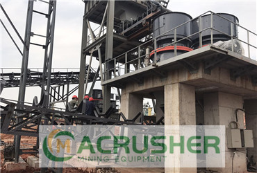
Knowing how to design a printed circuit board, PCB is a key element of any electronic circuit design process. The PCB layout and design has a major impact on the way in which a circuit work, and therefore if the printed circuit board is designed in an effective way, then the circuit will perform more reliably and within its specification. Typical complicated PCB design PCB design equipment
WhatsApp 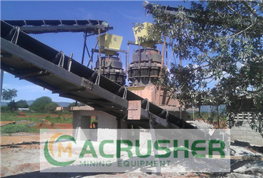
Owing to complicated structure of structure of multilayer PCBs, once problems are observed in the process of subsequent unit module assembly testing, it''s difficult to position breakdowns a result, inspection of their quality and reliability has to be very strict. Apart from regular inspection items mentioned above, other inspection items include the following parameters concerning
WhatsApp 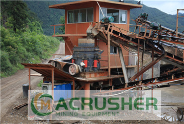
Circuit Technology Center, Inc. i s the world''s leading specialist in PC board repair and modification and the procedures described herein are the same procedures they use to repair and modify PC boards. They have been repairing PC boards for over 15 years for companies including Digital Equipment Corporation, IBM, Hewlett Packard, Siemens, Compaq Computer, ATT, Allied Signal Aerospace and
WhatsApp 
procedures to ensure the quality of their products. Inspection and testing pinpoint faulty boards for rework and provide process feedback that fuels continuous improvement. To maximize final yield and ultimate device reliability, each PCB needs to be inspected and tested based on its specific design and performance specifications. When a device OEM partners with a PCB
WhatsApp 
Printed circuit board assembly is a complex process, and there are possibilities of defects occurring in the process. Faults in PCB assembly can include failures in SMT equipment to incorrect component placement. Therefore, rigorous testing and inspection is crucial to ensure only the finest quality PCB products are delivered to the client.
WhatsApp 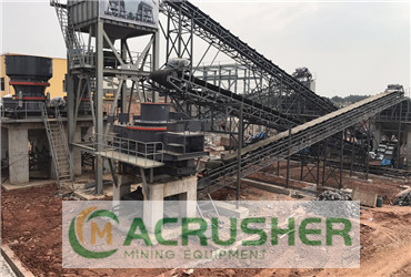
The best way to drill the holes out of a PCB board is to use a dremel, a 1/32 inch drill bit and it would be best to use a dremel press but if you cant do that you can clamp down the dremel and bring the board to the dremel by hand to drill the holes. Good luck and have fun!
WhatsApp The crushing and screen process is the crushing procedure composed of crushing machine and screening machine. The types of crushing process should be decided according to different crushing sections and different combinations of crusher and screen. The basic forms of crushing section are: single crushing operation, a crushing section with prescreening works, a crushing section with
WhatsApp The PCB crushing and separating machinery is used to process the separation of metal and nonmetal in waste printed circuit boards, copper clad laminate, circuit boards and leftover materials, then reuse the copper and resin powder. The equipment uses high voltage electrostatic separator to make the separation more fine, effectively control the loss of nonferrous metals. The separation rate of
WhatsApp 
PCB stands for "Printed circuit board". On this board all the components are soldered and interlinked by the copper tracks. The PCB can be a single layer and can go up to many layers as a person want, but most of the software support up to 14 layers. Most commonly used PCB is a single sided PCB and the components and conductors on different layers of PCB are connected with platedthrough
WhatsApp 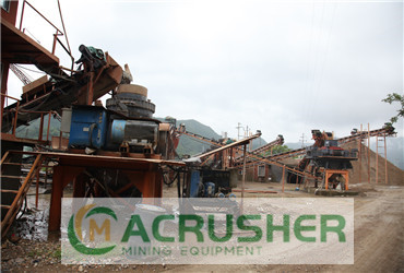
Being pulled into the crushing chamber when attempting to pull out contaminants ( reinforcing bar). Struck by the loader bucket if the access platform is within the working radius of the loading machine (for 360 degree excavators). Falling if adequate guardrails and access arrangements are not provided. Noise. Process noise at this level can cause deafness and adequate hearing protection
WhatsApp 06/01/2019· By establishing an appropriate PCB testing procedure for your organization''s needs, you can experience the benefits of PCB testing. What Is Being Tested? During the testing process, several components of PCBs are analyzed in detail, including: Lamination: Lamination quality is essential to the lifespan of a PCB — peeling laminate can cause issues in the final functionality of a board
WhatsApp  الصفحة الرئيسية
 معلومات عنا
 اتصل
اتصل